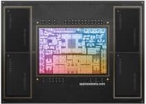
As the semiconductor industry leaps forward, TSMC is gearing up to introduce an extraordinary advancement in processor technology. The anticipated 1.6nm manufacturing process, heralded as a breakthrough, promises to significantly enhance the performance and efficiency of chips, particularly those used in Apple’s devices.
Nintendo Switch 2: Magnetic Innovations and Launch Insights
TSMC, a long-standing partner of Apple, has consistently been at the forefront of semiconductor innovation. Their new 1.6nm process is expected to follow the debut of Apple’s devices employing the 3nm node, showcasing TSMC’s commitment to pushing the boundaries of technology.
The new 1.6nm technology is poised to dramatically improve logic density, which is crucial for the miniaturization of future tech devices. With higher logic density, devices can perform more efficiently while consuming less power, a critical factor in mobile technology.
The anticipated benefits of the 1.6nm process include an 8-10% increase in speed and a 15-20% reduction in power consumption compared to its predecessors. This enhancement is pivotal for high-performance computing applications that require intensive processing capabilities without draining battery life.
Furthermore, TSMC’s innovative approach integrates nanosheet transistors with a novel back power rail solution. This combination not only enhances performance but also contributes to the compactness of the chip design, allowing more room for other essential components within a device.
Looking towards the future, TSMC has also revealed plans for even smaller node sizes, with trials for 2nm chips set to begin soon. These developments indicate a clear trajectory towards increasingly efficient and powerful semiconductor chips.
Apple, known for its high standards in product performance and quality, is likely to integrate these advanced chips into its future iPhone models. Rumors suggest that upcoming iPhone models will feature these cutting-edge chips, which will enhance everything from computing power to battery life.
In parallel with hardware advancements, TSMC is also pioneering the System-on-Wafer (SoW) technology. This innovative approach consolidates multiple dies on a single wafer, optimizing space and enhancing the computational power of the chips.
These technological strides by TSMC highlight the ongoing evolution in the semiconductor industry, driven by the demand for more powerful, efficient, and compact electronic devices. As these technologies mature and find their way into products, they have the potential to revolutionize not just smartphones but the entire spectrum of digital devices.
The ongoing partnership between TSMC and Apple underscores a mutual commitment to innovation and excellence in the tech industry. As we look towards 2026 and beyond, the fruits of this partnership are set to redefine the standards of what’s possible in technology.


